
Condensed Matter Physics
Semiconductors and Doping
Samuel J. Ling; Jeff Sanny; and William Moebs
Learning Objectives
By the end of this section, you will be able to:
- Describe changes to the energy structure of a semiconductor due to doping
- Distinguish between an n-type and p-type semiconductor
- Describe the Hall effect and explain its significance
- Calculate the charge, drift velocity, and charge carrier number density of a semiconductor using information from a Hall effect experiment
In the preceding section, we considered only the contribution to the electric current due to electrons occupying states in the conduction band. However, moving an electron from the valence band to the conduction band leaves an unoccupied state or hole in the energy structure of the valence band, which a nearby electron can move into. As these holes are filled by other electrons, new holes are created. The electric current associated with this filling can be viewed as the collective motion of many negatively charged electrons or the motion of the positively charged electron holes.
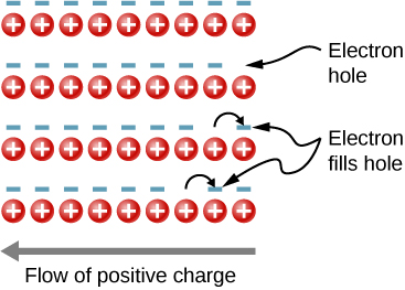
To illustrate, consider the one-dimensional lattice in (Figure). Assume that each lattice atom contributes one valence electron to the current. As the hole on the right is filled, this hole moves to the left. The current can be interpreted as the flow of positive charge to the left. The density of holes, or the number of holes per unit volume, is represented by p. Each electron that transitions into the conduction band leaves behind a hole. If the conduction band is originally empty, the conduction electron density p is equal to the hole density, that is,  .
.
As mentioned, a semiconductor is a material with a filled valence band, an unfilled conduction band, and a relatively small energy gap between the bands. Excess electrons or holes can be introduced into the material by the substitution into the crystal lattice of an impurity atom, which is an atom of a slightly different valence number. This process is known as doping. For example, suppose we add an arsenic atom to a crystal of silicon ((Figure)(a)).
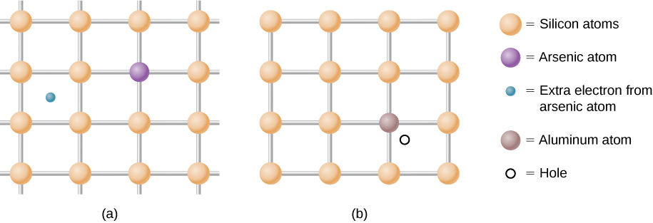
Arsenic has five valence electrons, whereas silicon has only four. This extra electron must therefore go into the conduction band, since there is no room in the valence band. The arsenic ion left behind has a net positive charge that weakly binds the delocalized electron. The binding is weak because the surrounding atomic lattice shields the ion’s electric field. As a result, the binding energy of the extra electron is only about 0.02 eV. In other words, the energy level of the impurity electron is in the band gap below the conduction band by 0.02 eV, a much smaller value than the energy of the gap, 1.14 eV. At room temperature, this impurity electron is easily excited into the conduction band and therefore contributes to the conductivity ((Figure)(a)). An impurity with an extra electron is known as a donor impurity, and the doped semiconductor is called an n-type semiconductor because the primary carriers of charge (electrons) are negative.
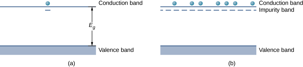
By adding more donor impurities, we can create an impurity band, a new energy band created by semiconductor doping, as shown in (Figure)(b). The Fermi level is now between this band and the conduction band. At room temperature, many impurity electrons are thermally excited into the conduction band and contribute to the conductivity. Conduction can then also occur in the impurity band as vacancies are created there. Note that changes in the energy of an electron correspond to a change in the motion (velocities or kinetic energy) of these charge carriers with the semiconductor, but not the bulk motion of the semiconductor itself.
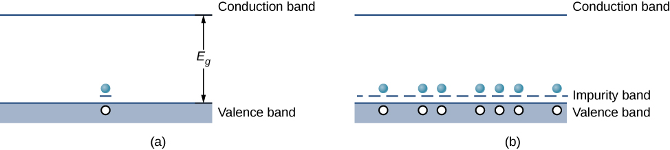
Doping can also be accomplished using impurity atoms that typically have one fewer valence electron than the semiconductor atoms. For example, Al, which has three valence electrons, can be substituted for Si, as shown in (Figure)(b). Such an impurity is known as an acceptor impurity, and the doped semiconductor is called a p-type semiconductor, because the primary carriers of charge (holes) are positive. If a hole is treated as a positive particle weakly bound to the impurity site, then an empty electron state is created in the band gap just above the valence band. When this state is filled by an electron thermally excited from the valence band ((Figure)(a)), a mobile hole is created in the valence band. By adding more acceptor impurities, we can create an impurity band, as shown in (Figure)(b).
The electric current of a doped semiconductor can be due to the motion of a majority carrier, in which holes are contributed by an impurity atom, or due to a minority carrier, in which holes are contributed purely by thermal excitations of electrons across the energy gap. In an n-type semiconductor, majority carriers are free electrons contributed by impurity atoms, and minority carriers are free electrons produced by thermal excitations from the valence to the conduction band. In a p-type semiconductor, the majority carriers are free holes contributed by impurity atoms, and minority carriers are free holes left by the filling of states due to thermal excitation of electrons across the gap. In general, the number of majority carriers far exceeds the minority carriers. The concept of a majority and minority carriers will be used in the next section to explain the operation of diodes and transistors.
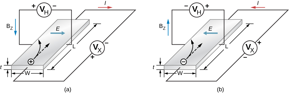
In studying p– and n-type doping, it is natural to ask: Do “electron holes” really act like particles? The existence of holes in a doped p-type semiconductor is demonstrated by the Hall effect. The Hall effect is the production of a potential difference due to the motion of a conductor through an external magnetic field (see The Hall Effect). A schematic of the Hall effect is shown in (Figure)(a). A semiconductor strip is bathed in a uniform magnetic field (which points into the paper). As the electron holes move from left to right through the semiconductor, a Lorentz force drives these charges toward the upper end of the strip. (Recall that the motion of the positively charged carriers is determined by the right-hand rule.) Positive charge continues to collect on the upper edge of the strip until the force associated with the downward electric field between the upper and lower edges of the strip  just balances the upward magnetic force
  . Setting these forces equal to each other, we have
  . The voltage that develops across the strip is therefore

where  is the Hall voltage; v is the hole’s drift velocity, or average velocity of a particle that moves in a partially random fashion; B is the magnetic field strength; and w is the width of the strip. Note that the Hall voltage is transverse to the voltage that initially produces current through the material. A measurement of the sign of this voltage (or potential difference) confirms the collection of holes on the top side of the strip. The magnitude of the Hall voltage yields the drift velocity (v) of the majority carriers.
Additional information can also be extracted from the Hall voltage. Note that the electron current density (the amount of current per unit cross-sectional area of the semiconductor strip) is

where q is the magnitude of the charge, n is the number of charge carriers per unit volume, and v is the drift velocity. The current density is easily determined by dividing the total current by the cross-sectional area of the strip, q is charge of the hole (the magnitude of the charge of a single electron), and u is determined by the Hall effect (Figure). Hence, the above expression for the electron current density gives the number of charge carriers per unit volume, n. A similar analysis can be conducted for negatively charged carriers in an n-type material (see (Figure)).
Summary
- The energy structure of a semiconductor can be altered by substituting one type of atom with another (doping).
- Semiconductor n-type doping creates and fills new energy levels just below the conduction band.
- Semiconductor p-type doping creates new energy levels just above the valence band.
- The Hall effect can be used to determine charge, drift velocity, and charge carrier number density of a semiconductor.
Conceptual Questions
What kind of semiconductor is produced if germanium is doped with (a) arsenic, and (b) gallium?
a. Germanium has four valence electrons. If germanium doped with arsenic (five valence electrons), four are used in bonding and one electron will be left for conduction. This produces an n-type material. b. If germanium is doped with gallium (three valence electrons), all three electrons are used in bonding, leaving one hole for conduction. This results in a p-type material.
What kind of semiconductor is produced if silicon is doped with (a) phosphorus, and (b) indium?
What is the Hall effect and what is it used for?
The Hall effect is the production of a potential difference due to motion of a conductor through an external magnetic field. This effect can be used to determine the drift velocity of the charge carriers (electrons or hole). If the current density is measured, this effect can also determine the number of charge carriers per unit volume.
For an n-type semiconductor, how do impurity atoms alter the energy structure of the solid?
For a p-type semiconductor, how do impurity atoms alter the energy structure of the solid?
It produces new unfilled energy levels just above the filled valence band. These levels accept electrons from the valence band.
Problems
An experiment is performed to demonstrate the Hall effect. A thin rectangular strip of semiconductor with width 10 cm and length 30 cm is attached to a battery and immersed in a 1.50-T field perpendicular to its surface. This produced a Hall voltage of 12 V. What is the drift velocity of the charge carriers?
Suppose that the cross-sectional area of the strip (the area of the face perpendicular to the electric current) presented to the in the preceding problem is  and the current is independently measured to be 2 mA. What is the number density of the charge carriers?

A current-carrying copper wire with cross-section  has a drift velocity of 0.02 cm/s. Find the total current running through the wire.
The Hall effect is demonstrated in the laboratory. A thin rectangular strip of semiconductor with width 5 cm and cross-sectional area  is attached to a battery and immersed in a field perpendicular to its surface. The Hall voltage reads 12.5 V and the measured drift velocity is 50 m/s. What is the magnetic field?
5 T
Glossary
- acceptor impurity
- atom substituted for another in a semiconductor that results in a free electron
- donor impurity
- atom substituted for another in a semiconductor that results in a free electron hole
- doping
- alteration of a semiconductor by the substitution of one type of atom with another
- drift velocity
- average velocity of a randomly moving particle
- hole
- unoccupied states in an energy band
- impurity atom
- acceptor or donor impurity atom
- impurity band
- new energy band create by semiconductor doping
- majority carrier
- free electrons (or holes) contributed by impurity atoms
- minority carrier
- free electrons (or holes) produced by thermal excitations across the energy gap
- n-type semiconductor
- doped semiconductor that conducts electrons
- p-type semiconductor
- doped semiconductor that conducts holes
