
Condensed Matter Physics
Semiconductor Devices
Samuel J. Ling; Jeff Sanny; and William Moebs
Learning Objectives
By the end of this section, you will be able to:
- Describe what occurs when n- and p-type materials are joined together using the concept of diffusion and drift current (zero applied voltage)
- Explain the response of a p-n junction to a forward and reverse bias voltage
- Describe the function of a transistor in an electric circuit
- Use the concept of a p-n junction to explain its applications in audio amplifiers and computers
Semiconductors have many applications in modern electronics. We describe some basic semiconductor devices in this section. A great advantage of using semiconductors for circuit elements is the fact that many thousands or millions of semiconductor devices can be combined on the same tiny piece of silicon and connected by conducting paths. The resulting structure is called an integrated circuit (ic), and ic chips are the basis of many modern devices, from computers and smartphones to the internet and global communications networks.
Diodes
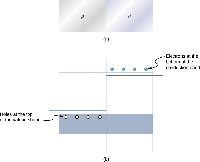
Perhaps the simplest device that can be created with a semiconductor is a diode. A diode is a circuit element that allows electric current to flow in only one direction, like a one-way valve (see Model of Conduction in Metals). A diode is created by joining a p-type semiconductor to an n-type semiconductor ((Figure)). The junction between these materials is called a p-n junction. A comparison of the energy bands of a silicon-based diode is shown in (Figure)(b). The positions of the valence and conduction bands are the same, but the impurity levels are quite different. When a p-n junction is formed, electrons from the conduction band of the n-type material diffuse to the p-side, where they combine with holes in the valence band. This migration of charge leaves positive ionized donor ions on the n-side and negative ionized acceptor ions on the p-side, producing a narrow double layer of charge at the p–n junction called the depletion layer. The electric field associated with the depletion layer prevents further diffusion. The potential energy for electrons across the p-n junction is given by (Figure).
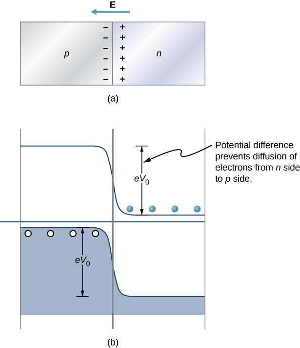
The behavior of a semiconductor diode can now be understood. If the positive side of the battery is connected to the n-type material, the depletion layer is widened, and the potential energy difference across the p-n junction is increased. Few or none of the electrons (holes) have enough energy to climb the potential barrier, and current is significantly reduced. This is called the reverse bias configuration. On the other hand, if the positive side of a battery is connected to the p-type material, the depletion layer is narrowed, the potential energy difference across the p-n junction is reduced, and electrons (holes) flow easily. This is called the forward bias configuration of the diode. In sum, the diode allows current to flow freely in one direction but prevents current flow in the opposite direction. In this sense, the semiconductor diode is a one-way valve.
We can estimate the mathematical relationship between the current and voltage for a diode using the electric potential concept. Consider N negatively charged majority carriers (electrons donated by impurity atoms) in the n-type material and a potential barrier V across the p-n junction. According to the Maxwell-Boltzmann distribution, the fraction of electrons that have enough energy to diffuse across the potential barrier is  . However, if a battery of voltage
  is applied in the forward-bias configuration, this fraction improves to
  . The electric current due to the majority carriers from the n-side to the p-side is therefore

where  is the current with no applied voltage and T is the temperature. Current due to the minority carriers (thermal excitation of electrons from the valence band to the conduction band on the p-side and subsequent attraction to the n-side) is
  , independent of the bias voltage. The net current is therefore

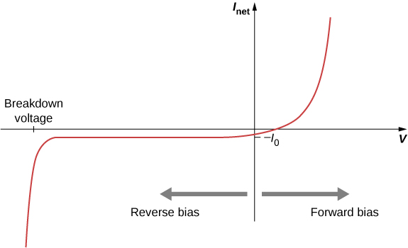
A sample graph of the current versus bias voltage is given in (Figure). In the forward bias configuration, small changes in the bias voltage lead to large changes in the current. In the reverse bias configuration, the current is  . For extreme values of reverse bias, the atoms in the material are ionized which triggers an avalanche of current. This case occurs at the breakdown voltage.
Diode Current Attaching the positive end of a battery to the p-side and the negative end to the n-side of a semiconductor diode produces a current of  The reverse saturation current is
  (The reverse saturation current is the current of a diode in a reverse bias configuration such as this.) The battery voltage is 0.12 V. What is the diode temperature?
Strategy The first arrangement is a forward bias configuration, and the second is the reverse bias configuration. In either case, (Figure) gives the current.
Solution The current in the forward and reverse bias configurations is given by
The current with no bias is related to the reverse saturation current by

Therefore

(Figure) can be written as

This ratio is much greater than one, so the second term on the left-hand side of the equation vanishes. Taking the natural log of both sides gives

The temperature is therefore

Significance The current moving through a diode in the forward and reverse bias configuration is sensitive to the temperature of the diode. If the potential energy supplied by the battery is large compared to the thermal energy of the diode’s surroundings,  then the forward bias current is very large compared to the reverse saturation current.
Check Your Understanding How does the magnitude of the forward bias current compare with the reverse bias current?
The forward bias current is much larger. To a good approximation, diodes permit current flow in only one direction.
Create a p–n junction and observe the behavior of a simple circuit for forward and reverse bias voltages. Visit this site to learn more about semiconductor diodes.
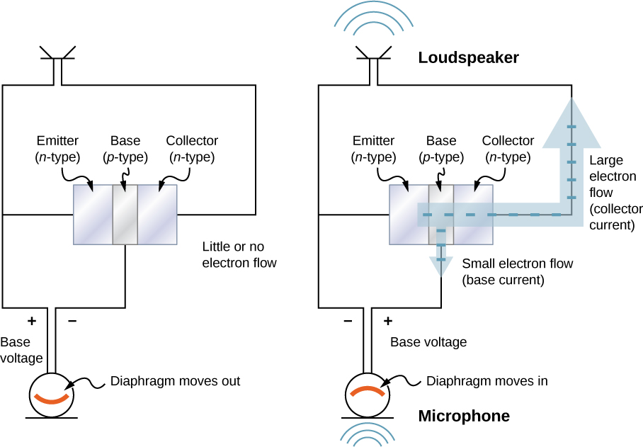
Junction Transistor
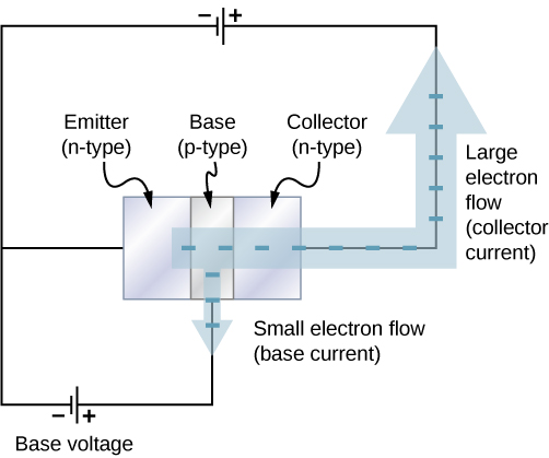
If diodes are one-way valves, transistors are one-way valves that can be carefully opened and closed to control current. A special kind of transistor is a junction transistor. A junction transistor has three parts, including an n-type semiconductor, also called the emitter; a thin p-type semiconductor, which is the base; and another n-type semiconductor, called the collector ((Figure)). When a positive terminal is connected to the p-type layer (the base), a small current of electrons, called the base current  flows to the terminal. This causes a large collector current
  to flow through the collector. The base current can be adjusted to control the large collector current. The current gain is therefore

A junction transistor can be used to amplify the voltage from a microphone to drive a loudspeaker. In this application, sound waves cause a diaphragm inside the microphone to move in and out rapidly ((Figure)). When the diaphragm is in the “in” position, a tiny positive voltage is applied to the base of the transistor. This opens the transistor “valve” and allows a large electrical current flow to the loudspeaker. When the diaphragm is in the “out” position, a tiny negative voltage is applied to the base of the transistor, which shuts off the transistor valve so that no current flows to the loudspeaker. This shuts the transistor “valve” off so no current flows to the loudspeaker. In this way, current to the speaker is controlled by the sound waves, and the sound is amplified. Any electric device that amplifies a signal is called an amplifier.
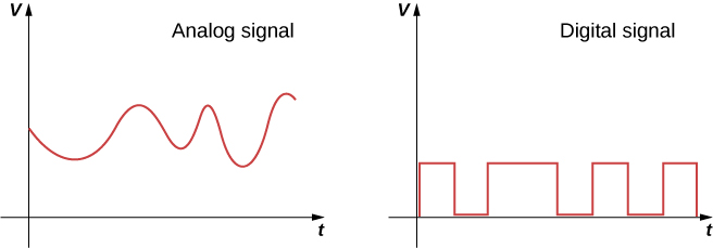
In modern electronic devices, digital signals are used with diodes and transistors to perform tasks such as data manipulation. Electric circuits carry two types of electrical signals: analog and digital ((Figure)). An analog signal varies continuously, whereas a digital signal switches between two fixed voltage values, such as plus 1 volt and zero volts. In digital circuits like those found in computers, a transistor behaves like an on-off switch. The transistor is either on, meaning the valve is completely open, or it is off, meaning the valve is completely closed. Integrated circuits contain vast collections of transistors on a single piece of silicon. They are designed to handle digital signals that represent ones and zeroes, which is also known as binary code. The invention of the ic helped to launch the modern computer revolution.
Summary
- A diode is produced by an n-p junction. A diode allows current to move in just one direction. In forward biased configuration of a diode, the current increases exponentially with the voltage.
- A transistor is produced by an n-p-n junction. A transistor is an electric valve that controls the current in a circuit.
- A transistor is a critical component in audio amplifiers, computers, and many other devices.
Conceptual Questions
When p– and n-type materials are joined, why is a uniform electric field generated near the junction?
When p– and n-type materials are joined, why does the depletion layer not grow indefinitely?
The electric field produced by the uncovered ions reduces further diffusion. In equilibrium, the diffusion and drift currents cancel so the net current is zero. Therefore, the resistance of the depletion region is large.
How do you know if a diode is in the forward biased configuration?
Why does the reverse bias configuration lead to a very small current?
The positive terminal is applied to the n-side, which uncovers more ions near the junction (widens the depletion layer), increases the junction voltage difference, and therefore reduces the diffusion of holes across the junction.
What happens in the extreme case that where the n– and p-type materials are heavily doped?
Explain how an audio amplifier works, using the transistor concept.
Sound moves a diaphragm in and out, which varies the input or base current of the transistor circuit. The transistor amplifies this signal (p-n-p semiconductor). The output or collector current drives a speaker.
Problems
Show that for V less than zero, 
A p-n diode has a reverse saturation current  . It is forward biased so that it has a current of
  moving through it. What bias voltage is being applied if the temperature is 300 K?

The collector current of a transistor is 3.4 A for a base current of 4.2 mA. What is the current gain?
Applying the positive end of a battery to the p-side and the negative end to the n-side of a p-n junction, the measured current is  . Reversing this polarity give a reverse saturation current of
  . What is the temperature if the bias voltage is 1.2 V?

The base current of a transistor is 4.4 A, and its current gain 1126. What is the collector current?
Glossary
- amplifier
- electrical device that amplifies an electric signal
- base current
- current drawn from the base n-type material in a transistor
- breakdown voltage
- in a diode, the reverse bias voltage needed to cause an avalanche of current
- collector current
- current drawn from the collector p-type material
- depletion layer
- region near the p-n junction that produces an electric field
- forward bias configuration
- diode configuration that results in high current
- junction transistor
- electrical valve based on a p-n-p junction
- p-n junction
- junction formed by joining p– and n-type semiconductors
- reverse bias configuration
- diode configuration that results in low current
