Condensed Matter Physics
Band Theory of Solids
Samuel J. Ling; Jeff Sanny; and William Moebs
Learning Objectives
By the end of this section, you will be able to:
- Describe two main approaches to determining the energy levels of an electron in a crystal
- Explain the presence of energy bands and gaps in the energy structure of a crystal
- Explain why some materials are good conductors and others are good insulators
- Differentiate between an insulator and a semiconductor
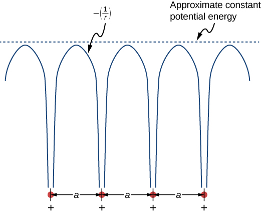
The free electron model explains many important properties of conductors but is weak in at least two areas. First, it assumes a constant potential energy within the solid. (Recall that a constant potential energy is associated with no forces.) (Figure) compares the assumption of a constant potential energy (dotted line) with the periodic Coulomb potential, which drops as ![]() at each lattice point, where r is the distance from the ion core (solid line). Second, the free electron model assumes an impenetrable barrier at the surface. This assumption is not valid, because under certain conditions, electrons can escape the surface—such as in the photoelectric effect. In addition to these assumptions, the free electron model does not explain the dramatic differences in electronic properties of conductors, semiconductors, and insulators. Therefore, a more complete model is needed.
at each lattice point, where r is the distance from the ion core (solid line). Second, the free electron model assumes an impenetrable barrier at the surface. This assumption is not valid, because under certain conditions, electrons can escape the surface—such as in the photoelectric effect. In addition to these assumptions, the free electron model does not explain the dramatic differences in electronic properties of conductors, semiconductors, and insulators. Therefore, a more complete model is needed.

We can produce an improved model by solving Schrödinger’s equation for the periodic potential shown in (Figure). However, the solution requires technical mathematics far beyond our scope. We again seek a qualitative argument based on quantum mechanics to find a way forward.
We first review the argument used to explain the energy structure of a covalent bond. Consider two identical hydrogen atoms so far apart that there is no interaction whatsoever between them. Further suppose that the electron in each atom is in the same ground state: a 1s electron with an energy of ![]() (ignore spin). When the hydrogen atoms are brought closer together, the individual wave functions of the electrons overlap and, by the exclusion principle, can no longer be in the same quantum state, which splits the original equivalent energy levels into two different energy levels. The energies of these levels depend on the interatomic distance,
(ignore spin). When the hydrogen atoms are brought closer together, the individual wave functions of the electrons overlap and, by the exclusion principle, can no longer be in the same quantum state, which splits the original equivalent energy levels into two different energy levels. The energies of these levels depend on the interatomic distance, ![]() ((Figure)).
((Figure)).
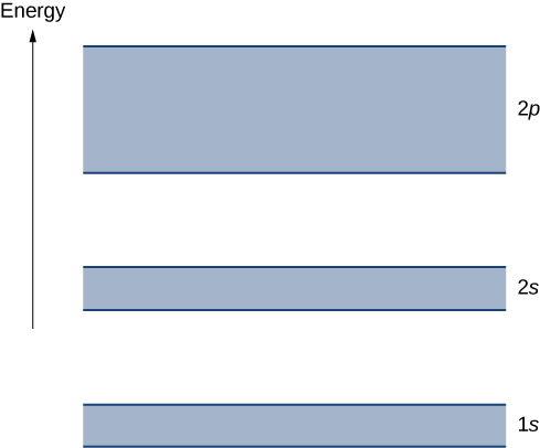
If four hydrogen atoms are brought together, four levels are formed from the four possible symmetries—a single sine wave “hump” in each well, alternating up and down, and so on. In the limit of a very large number N of atoms, we expect a spread of nearly continuous bands of electronic energy levels in a solid (see (Figure)(c)). Each of these bands is known as an energy band. (The allowed states of energy and wave number are still technically quantized, but for large numbers of atoms, these states are so close together that they are consider to be continuous or “in the continuum.”)
Energy bands differ in the number of electrons they hold. In the 1s and 2s energy bands, each energy level holds up to two electrons (spin up and spin down), so this band has a maximum occupancy of 2N electrons. In the 2p energy band, each energy level holds up to six electrons, so this band has a maximum occupancy of 6N electrons ((Figure)).


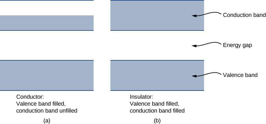
Each energy band is separated from the other by an energy gap. The electrical properties of conductors and insulators can be understood in terms of energy bands and gaps. The highest energy band that is filled is known as a valence band. The next available band in the energy structure is known as a conduction band. In a conductor, the highest energy band that contains electrons is partially filled, whereas in an insulator, the highest energy band containing electrons is completely filled. The difference between a conductor and insulator is illustrated in (Figure).
A conductor differs from an insulator in how its electrons respond to an applied electric field. If a significant number of electrons are set into motion by the field, the material is a conductor. In terms of the band model, electrons in the partially filled conduction band gain kinetic energy from the electric field by filling higher energy states in the conduction band. By contrast, in an insulator, electrons belong to completely filled bands. When the field is applied, the electrons cannot make such transitions (acquire kinetic energy from the electric field) due to the exclusion principle. As a result, the material does not conduct electricity.

Visit this simulation to learn about the origin of energy bands in crystals of atoms and how the structure of bands determines how a material conducts electricity. Explore how band structure creates a lattice of many wells.
A semiconductor has a similar energy structure to an insulator except it has a relatively small energy gap between the lowest completely filled band and the next available unfilled band. This type of material forms the basis of modern electronics. At ![]() , the semiconductor and insulator both have completely filled bands. The only difference is in the size of the energy gap (or band gap) Eg between the highest energy band that is filled (the valence band) and the next-higher empty band (the conduction band). In a semiconductor, this gap is small enough that a substantial number of electrons from the valence band are thermally excited into the conduction band at room temperature. These electrons are then in a nearly empty band and can respond to an applied field. As a general rule of thumb, the band gap of a semiconductor is about 1 eV. (See (Figure) for silicon.) A band gap of greater than approximately 1 eV is considered an insulator. For comparison, the energy gap of diamond (an insulator) is several electron-volts.
, the semiconductor and insulator both have completely filled bands. The only difference is in the size of the energy gap (or band gap) Eg between the highest energy band that is filled (the valence band) and the next-higher empty band (the conduction band). In a semiconductor, this gap is small enough that a substantial number of electrons from the valence band are thermally excited into the conduction band at room temperature. These electrons are then in a nearly empty band and can respond to an applied field. As a general rule of thumb, the band gap of a semiconductor is about 1 eV. (See (Figure) for silicon.) A band gap of greater than approximately 1 eV is considered an insulator. For comparison, the energy gap of diamond (an insulator) is several electron-volts.
| Material | Energy Gap |
|---|---|
Summary
- The energy levels of an electron in a crystal can be determined by solving Schrödinger’s equation for a periodic potential and by studying changes to the electron energy structure as atoms are pushed together from a distance.
- The energy structure of a crystal is characterized by continuous energy bands and energy gaps.
- The ability of a solid to conduct electricity relies on the energy structure of the solid.
Conceptual Questions
What are the two main approaches used to determine the energy levels of electrons in a crystal?
(1) Solve Schrödinger’s equation for the allowed states and energies. (2) Determine energy levels for the case of a very large lattice spacing and then determine the energy levels as this spacing is reduced.
Describe two features of energy levels for an electron in a crystal.
How does the number of energy levels in a band correspond to the number, N, of atoms.
For N atoms spaced far apart, there are N different wave functions, all with the same energy (similar to the case of an electron in the double well of ![]() As the atoms are pushed together, the energies of these N different wave functions are split. By the exclusion principle, each electron must each have a unique set of quantum numbers, so the N atoms bringing N electrons together must have at least N states.
As the atoms are pushed together, the energies of these N different wave functions are split. By the exclusion principle, each electron must each have a unique set of quantum numbers, so the N atoms bringing N electrons together must have at least N states.
Why are some materials very good conductors and others very poor conductors?
Why are some materials semiconductors?
For a semiconductor, there is a relatively large energy gap between the lowest completely filled band and the next available unfilled band. Typically, a number of electrons traverse the gap and therefore the electrical conductivity is small. The properties of a semiconductor are sensitivity to temperature: As the temperature is increased, thermal excitations promote charge carriers from the valence band across the gap and into the conduction band.
Why does the resistance of a semiconductor decrease as the temperature increases?
Problems
For a one-dimensional crystal, write the lattice spacing (a) in terms of the electron wavelength.
What is the main difference between an insulator and a semiconductor?
For an insulator, the energy gap between the valence band and the conduction band is larger than for a semiconductor.
What is the longest wavelength for a photon that can excite a valence electron into the conduction band across an energy gap of 0.80 eV?
A valence electron in a crystal absorbs a photon of wavelength, ![]() . This is just enough energy to allow the electron to jump from the valence band to the conduction band. What is the size of the energy gap?
. This is just enough energy to allow the electron to jump from the valence band to the conduction band. What is the size of the energy gap?
4.13 keV
Glossary
- conduction band
- above the valence band, the next available band in the energy structure of a crystal
- energy band
- nearly continuous band of electronic energy levels in a solid
- energy gap
- gap between energy bands in a solid
- semiconductor
- solid with a relatively small energy gap between the lowest completely filled band and the next available unfilled band
- valence band
- highest energy band that is filled in the energy structure of a crystal

